- This topic is empty.
-
AuthorPosts
-
2026-11-10 at 5:02 pm #12981
Understanding Tombstoning in Surface-Mount Assembly
Tombstoning is a well-recognized defect in surface-mount technology (SMT) assembly. It occurs when a small two-terminal component—typically a chip resistor or chip capacitor—lifts off one solder pad during reflow and rotates upward, ending up standing on one end like a miniature tombstone rather than lying flat across both pads. The result is an open circuit, a failed electrical connection, and a board that must be reworked or scrapped before it ever reaches functional testing. For engineers designing compact modules with densely packed small components, understanding why tombstoning happens—and where in the design-to-assembly chain it can be prevented—is essential.
Primary Causes of Tombstoning During Reflow
Tombstoning is fundamentally a wetting-force imbalance problem. During reflow, solder paste on each pad melts and generates surface tension that pulls the component terminal toward the pad. If the pulling force on one side becomes significantly stronger or happens earlier than on the other side, the component can be lifted and rotated before the second joint solidifies. Several design and process factors contribute to this imbalance.
Pad and Footprint Design Imbalance
Asymmetric pad geometry is one of the most common root causes. If the two pads for a small chip component are not identical in size, shape, or copper thermal relief, one pad will reach reflow temperature and develop wetting force before the other. Differences in trace width connecting to each pad, or one pad being tied to a larger copper plane that acts as a heat sink while the other is isolated, can create exactly this kind of thermal and wetting asymmetry.
Uneven Solder Paste Volume
Inconsistent stencil aperture design or uneven paste deposition between the two pads of a component can also upset the balance of wetting forces. A pad with more paste volume generates stronger surface tension pull during melt, increasing the likelihood that the opposite end lifts first.
Reflow Thermal Profile Asymmetry
Even with balanced pad design, an uneven thermal profile across the board—caused by component density, nearby thermal mass, or oven zone variation—can cause one side of a small component to reach liquidus temperature before the other. This timing gap is often enough to trigger tombstoning, particularly for very small passive components where the self-weight is too low to resist the asymmetric pull.
Component Placement and Polarity Misalignment
Placement accuracy also plays a role. A component that is slightly offset from its intended footprint may rest unevenly on the paste deposits, altering how each terminal wets during reflow. For polarized or orientation-sensitive parts, misalignment compounds the risk, since uneven paste contact area on each terminal changes the wetting force balance in the same way that pad or paste asymmetry does.
Why Prevention Starts Before Fabrication
Because tombstoning results from the interaction of pad design, paste volume, thermal behavior, and placement accuracy, it cannot be reliably solved by adjusting the reflow oven alone. Many of the underlying causes are set earlier—at the footprint design stage and in the assembly file preparation stage—well before the board reaches the reflow line. This is why engineering review of Gerbers, BOM, and placement data before fabrication begins is widely regarded as a more effective control point than attempting to correct the issue after boards have already been built and populated.
How GreatPCB’s Engineering Review Addresses Tombstoning Risk
GreatPCB positions its service specifically around this principle: performing engineering review before production begins, rather than discovering file inconsistencies or footprint problems after assembly. For LED and other small-component modules, GreatPCB’s process includes LED footprint and polarity review, in which pad dimensions, orientation, and polarity marks are compared against the component datasheet and assembly drawing before fabrication files are released. This same review logic—checking that pad geometry and placement data are consistent and match the component’s actual footprint requirements—is the type of check that helps catch footprint asymmetries and placement data errors that can contribute to wetting-force imbalance during reflow.
GreatPCB’s broader file consistency review also cross-checks board number, revision, polarity, and reference designators across Gerbers, drill files, BOM, placement coordinates, and assembly drawings, raising a query with the customer whenever placement orientation conflicts with the assembly drawing. For boards with densely populated small components, this consistency check reduces the chance that a placement or footprint discrepancy makes it into fabrication undetected.
In addition, GreatPCB’s assembly and inspection alignment step agrees on inspection scope—and, where required, power-up procedure and functional test criteria—before assembly runs. This gives both the manufacturer and the customer a defined point at which placement accuracy and joint quality, including any tombstoning or lifted-component conditions, would be identified through inspection rather than discovered later in the field.
From Design File to Assembled Module: A Traceable Process
GreatPCB’s DFM review is performed after the customer confirms Gerbers, BOM, and assembly information, establishing traceable file revisions for both prototype and later production orders. Delivery includes board and revision identification, a quantity list, and applicable inspection or test records, so that any assembly-stage finding—including issues related to component placement—can be tied back to a specific, documented revision rather than left ambiguous. GreatPCB’s current demonstrated delivery capability covers low-volume prototype builds, either as bare boards or as assembled modules, depending on the order agreement.
This traceability matters directly for tombstoning risk management. When a defect is found during inspection, having documented revisions of the footprint, BOM, and placement coordinates allows the actual cause—whether a pad design choice, a paste or placement variable, or a thermal profile issue—to be isolated and addressed in the next revision rather than guessed at after the fact.
Conclusion
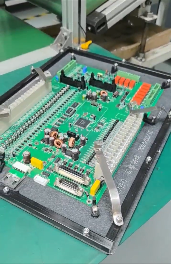
Tombstoning during reflow is caused by an imbalance of wetting forces between a small component’s two terminals, driven by asymmetric pad design, uneven solder paste volume, reflow thermal profile differences, or placement misalignment. Because these variables are largely determined before a board is ever assembled, catching them through engineering review of footprint geometry, file consistency, and placement data offers a more direct path to prevention than reacting after assembly. GreatPCB’s pre-production engineering review—covering footprint and polarity verification, cross-file consistency checks, and defined inspection alignment—reflects this design-stage approach, giving manufacturers of LED modules and other small-component assemblies a documented, traceable basis for addressing placement and footprint issues before they translate into reflow defects.
GreatPCB -
AuthorPosts

- You must be logged in to reply to this topic.